
Now on factory floors: Ultra-precise chip etching technology enabled by NSF-funded plasma science
How a 10-year partnership between NSF, industry and academia gave a U.S. company an edge in the competitive global semiconductor production market
Earlier this year, Lam Research, a U.S.-based maker of semiconductor fabrication equipment, unveiled a new product that can reliably mass produce the exquisitely complex circuits required for future electronic applications, particularly those involving artificial intelligence. This new technology got its start a decade ago in a UCLA lab with a small team of scientists supported by a partnership between the U.S. National Science Foundation and Lam Research.
At the heart of the technology is a method that can more precisely control plasma — the electrically charged state of matter that makes semiconductor etching machines work.
"To enable the growth of AI-capable consumer electronics, future semiconductor device architectures will require precise plasma etching capabilities that exceed today's most advanced technologies," says Alex Paterson, Lam Research corporate vice president for etch products.
Paterson says Lam Research's new precision-etching technology, which they market under the name DirectDrive ®, exceeds current technologies with its ability to etch smaller, denser and 3D semiconductor devices with angstrom-level precision (for perspective, a single hydrogen atom is about one angstrom wide).
"The DirectDrive project started from the seed program, where we had valuable collaboration with NSF," says Paterson of the partnership created through the NSF Grant Opportunities for Academic Liaison with Industry (GOALI) program which promotes cooperation between research institutions and industry to conduct scientific and engineering work specifically aimed at creating breakthrough technologies for U.S. industry.

DirectDrive is already being used in Lam's latest plasma etch tools to crank out advanced circuits in the spotlessly dust-free clean rooms of chip manufacturing facilities. But, the commercial viability of the method required years of meticulous scientific work — and it all began in one guy's home kitchen.
From kitchen to lab
"There is a square inch of silicon manufactured for every person on the planet every year," says UCLA engineer Patrick Pribyl on the immensity of the global, silicon-based semiconductor industry.
In 2006, Pribyl created a prototype for a new way to control plasma etching. He made it in a makeshift lab in his kitchen. Although he shopped his invention around to industrial etching machine companies at the time, he couldn't get any traction because of the daunting scientific work needed to bridge the technological canyon between kitchen prototype and market.

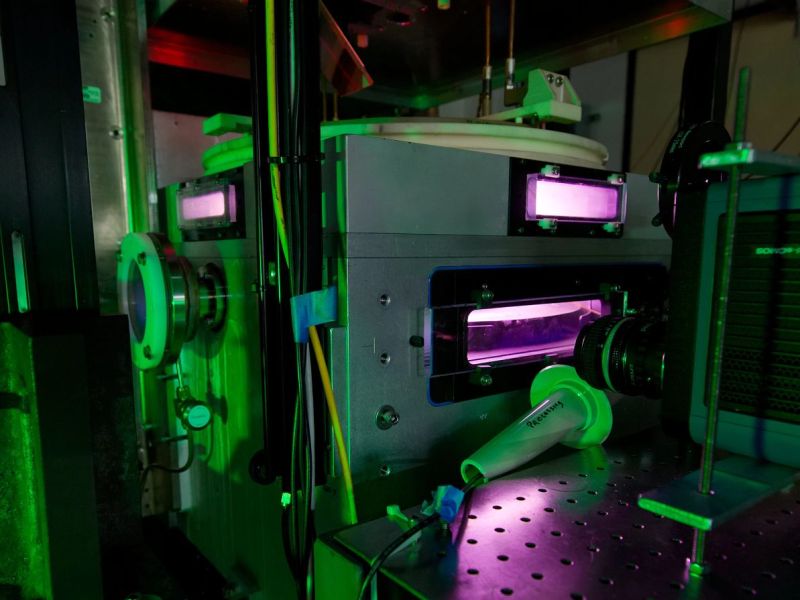
Undeterred, Pribyl teamed up with physicist Walter Gekelman, director of the UCLA Basic Plasma Science Facility. Together, they secured GOALI funding from NSF in 2015 to pursue the science and Lam Research donated an industrial plasma etching machine and other equipment. Pribyl and Gekelman got to work stripping down and modifying Lam's machine to see if their method really could change the way chips are manufactured.
"We realized early on how important this was for industry," says Gekelman of their belief in what the new method could achieve if brought to market.
Their eventual results were met with disbelief. "They said 'that's impossible,'" remembers Pribyl of the initial reactions from others in the industry. "It just dumbfounded the semiconductor community that this could be done."
The limiting factor in creating more advanced chips is the smallest size at which nanometer-sized electronic components can be etched reliably enough to work. Faster, more powerful chips require tinier and more intricate features.
The crux of Pribyl's method is a simplified process to rapidly switch — or "pulse" — radio frequency electrical energy that creates and drives the plasma inside semiconductor etching machines. At relatively low power, radio frequency energy (commonly referred to as "RF" energy) can wirelessly transmit data like text messages and streaming movies. At higher power levels, it can create the electrically charged form of matter known as plasma. RF energy is commonly used to partially ionize the chemical mixtures inside etching machines, changing them from gas into plasma. The charged particles of the plasma then rain down on the silicon and eat away at the carefully unmasked areas of the chip, leaving behind intricate, tiny circuits.
To understand the role of RF energy switching in semiconductor etching, imagine a sculptor switching between chisels of different shapes and sizes when carving a block of marble. The sculptor might use a certain chisel for chipping away big chunks of marble and switch to a different one for carving delicate features. Similarly, the RF energy used to generate the plasma inside an etching machine must be regularly stopped, started and changed to control the power of the plasma and the depth of the etching.
Unlike the sculptor who can simply stop hammering their chisel when they want to switch tools, the plasma keeps "chiseling" the silicon for several seconds while the RF energy is mechanically switched to a different power level. However, the fast-switching method can turn the power on or off within 50 microseconds — less than one ten-thousandth of the time previously required.
By rapidly pulsing the RF energy thousands of times per second — which is what DirectDrive does — the plasma can be controlled far more precisely and can thus reliably etch smaller electronic components. Lam Research found their etching process was greatly improved after incorporating the pulsed plasma technology.
From lab to factory floor
"In the early 2010s, Lam Research examined the needs and requirements for plasma delivery technologies to empower future semiconductor processing," says Paterson. "None of the alternatives on the market at that time were meeting the stringent demands of speed, power, precision, reliability and form factor. As a result, Lam shifted its approach to product development by leveraging new ideas and methodologies from academia."
DirectDrive is an example of this partnership with academic researchers, explains Paterson.
The breakthrough didn't happen overnight, though. Like so many scientific projects, it took years of painstaking experiments and precise measurements in the lab. "Essentially what we do is devise experiments and make measurements," says Gekelman.
And, adds Pribyl, "We can do it way better than what can be done on a factory floor."
Gekelman, Pribyl and Paterson spent nearly 10 years in the UCLA lab using lasers and a custom-made probe to observe the complex, 3D movement of ions in the pulsed plasma, along with properties like density, temperature, and electric and magnetic fields.

"We also measured how fast the ions are going," says Gekelman. "If they're moving straight down or a little sideways, and if the angle they're hitting the wafer is the same everywhere on the wafer."
Their exhaustive measurements yielded a fuller understanding of the fundamental nature of plasma and provided the rigorous scientific basis needed to scale-up the pulsed plasma process to an industrial level. Gekelman and Pribyl's collaborators at the University of Michigan further contributed by using computer modeling to simulate the plasma's behavior in areas of the machine that could not be directly observed in the UCLA lab.
"Beyond the results and breakthroughs that provide us with new understanding of nature and the basis for new technologies, labs like these are the pipeline for attracting and training scientists and engineers who can propel U.S. industry with their ideas," says Vyacheslav (Slava) Lukin, program director for the NSF Plasma Physics program. "Students from these labs are oftentimes recruited by industry before they even begin to write their Ph.D. theses."
Behind each inflection in semiconductor technology are years of development backed by more years of scientific research, says Paterson.
"This cycle of collaboration and innovation is what propels the industry forward."